


Working with Microchip PIC 8-bit GPIO
This third in a series of five articles exploring getting started with development on the Microchip PIC 8-bit family of processors focuses on basic GPIO (General Purpose Input Output). The initial post looked at some of the Microchip hardware options for getting started with the PIC 8-bit development, discussed Microchip development tools, and wrapped up with setting up a basic project using the GUI based MPLAB Code Configurator (MCC) plug-in. The second post picked up with a basic review of memory architecture and organization of the 8-bit PIC family, processor initialization elements, and closed with a walk through of the MCC generated file structure and code to gain a better understanding of the oscillator and clock configuration code. This getting started series focuses on the PIC 8-bit High-End Family, specifically the PIC18F47Q10 processor. This post, like the first post, uses a discrete PIC18F47Q10 processor in a PDIP40 package using an MPLAB PICkit 4 programmer / debugger; however, ports and pins were selected such that the Curiosity High Pin Count development board can be used with the same code base. This GPIO exploration looks into the following areas:
- 8-bit PIC GPIO Ports
- 8-bit PIC GPIO Registers
- Breadboarding the External Components
- Creating the MPLAB X Project
- Coding to Flash LEDs
The completed code for this post can be downloaded from GitHub here.
PIC®, MPLAB® X, and PICkit™ 4 are trademarks of Microchip Technology Inc.
All data sheet references are to Microchip document PIC18F27_47Q10-data-sheet-40002043C, © 2019 - Microchip Technology Inc, available here at the time this post was published.
PIC GPIO Ports
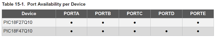
The PIC18F47Q10 datasheet covers GPIO in section 15, I/O Ports. A key construct / unit of organization when discussing GPIO is the port. Many processor families, Microchip PIC included, use the concept of a port to map physical processor pins to individual memory registers (SFRs - Special Function Registers) with one pin mapping to one bit in an 8-bit register. Therefore, each port represents at most eight physical pins for an 8-bit processor architecture. Further, the concept of port also encompasses the various SFRs used to manage and interact with physical pins. From the datasheet, the 8-bit PIC family provides a total of eight registers for managing a single port. Like most processor platforms – the PIC platform uses letters for identifying each port, the datasheet indicates there are five ports available on the PIC18F47Q10 – labeled A-E.
Physical Packaging
The PIC18F47Q10 chip used in this post is available in a PDIP40 package. A PDIP40 package has 40 physical pins available; five ports of 8 pins would take up all the 40 available pins. However, the processor needs dedicated pins for VDD and VSS (typically 2 or more pins for each), one or more pins for programming, a reset pin, etc. So clearly, a 40-pin package is not able to dedicate physical pins to all the logical pins from five 8-bit ports. Additionally, GPIO is not the only peripheral the PIC18F47Q10 supports – physical pins are needed for external interrupts, communications (serial, I2C, SPI), timer outputs, A/D conversion, etc. Basically any peripheral that interacts with the “world” outside of the physical processor requires some number of physical pins. Each port supports mapping pins of the various port to different peripherals. For one application, pin RC7 can be configured as the Rx pin for the Serial Port 1, while in another application the same RC7 pin can be configured as a GPIO output pin.
The MPLAB X IDE provides a pin out diagram for this package (the pin out is also available in the datasheet).
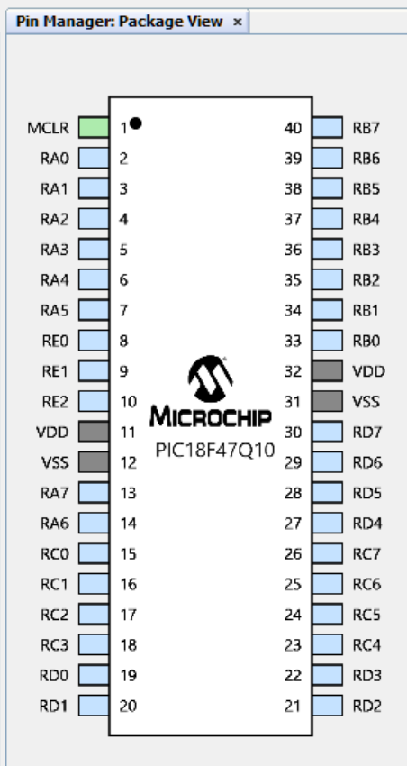
From the above diagram, PortA, PortB, PortC and PortD have all eight pins / bits available, while PortE has only three pins available.
Port Pin Mapping
As mentioned previously, the PIC18F47Q10 (and the PIC processor
line in general) implements a physical pin sharing scheme allowing
a pin to be configured for various functions. The mapping
available for each pin is available in the processor datasheet
introduction - Pin Allocation Tables. There are individual
tables for the different physical packages - the 40-pin package is
covered in Table 4. A subsection of that table showing the
available port B mappings appears as:
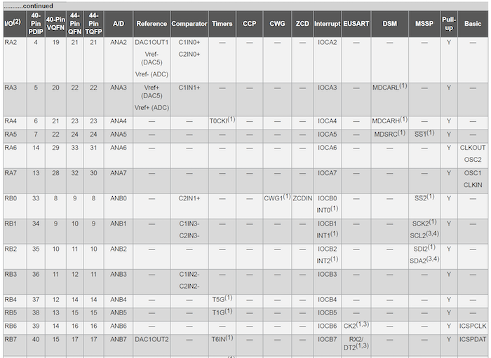
Looking at the table Port B / pin 2 (RB2) can be allocated for
A/D (Analog / Digital converter), external interrupts, or the MSSP
(Master Synchronous Serial Port – SPI / I2C). How this
configuration is managed for other than GPIO in outside of the
scope of this discussion.
PIC GPIO Registers
The 8-bit PIC® PIC18F47Q10 has five available ports with eight registers
associated with each port. The eight registers are:
- PORTx
- LATx
- TRISx
- ANSELx
- WPUx
- INLVLx
- SLRCONx
- ODCONx
In this post port (lowercase) refers to the broader concept as it applies to the microcontroller pin grouping, while PORT (uppercase) refers to the actual SFR.
Each register, such as the PORT register, behaves identically regardless of port (A through E), however, each port has a unique SFR address. This is why the each of the registers listed above has an ‘x’ suffix – simply replace the ‘x’ with the port letter of interest, e.g. PORTA, PORTD, etc. The symbols for the various registers are defined in the processor specific include file, in this case, pic18f47q10.h, discussed in the second post of this series.
The various registers work together to determine the direction
of each pin in the port: input vs output, whether weak
internal pull up resistors are enabled, whether the pin is used as
part of an analog module which in turn determines if the voltages on the pin are treated as analog
or digital values, etc. The digital logic implementation behind
each pin is not a simple direction connection to an internal bus
but connection to the bus is through a non-trivial set of digital
components. The processor datasheet provides details of the
actual I/O port implementation:
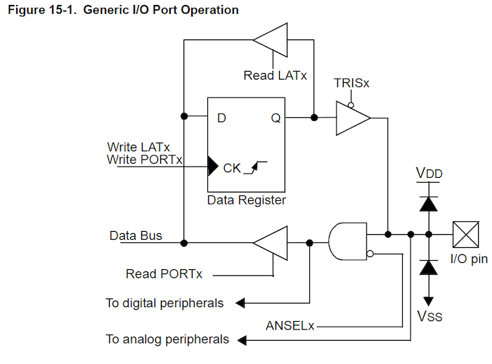
TRIS Register
The TRISx (TRIState) register determines whether the associated pin is input (logic high) or output (logic low). Each TRISx bit value drives the select bit of the output buffer (driver) in the above diagram – the bubble on the select line indicates the buffer is enabled when the select line is logic level low. Upon processor reset, the TRISx registers default to 0xFF – output drivers disabled. The pins of the port can be configured individually.
PORT and LAT Register
The PORTx and LATx (LATch) registers are the mechanism for reading and writing pin values. The LATx port is a digital LATch holding the last value written to the register / pin, note from the diagram above the writing / reading the LATx register never directly affects the physical pin. As port write operations are read-modify-write operations, the latch provides protection for possible errors that can occur when writing output values to the port. Microchip recommends using the associated LATx register for pin operations when the pin is configured as output and the PORTx register for reading pin values when the pin is configured as an input.
The following annotated diagrams help to clarify how values are
read and written for a pin with the PORTx and LATx registers.
PORTx Read
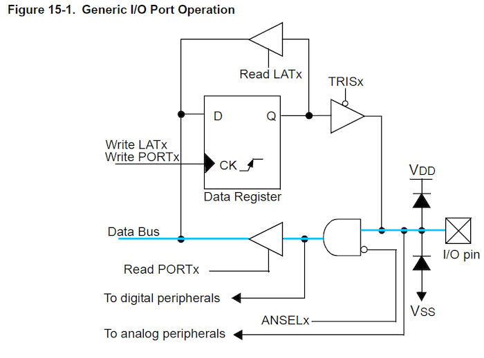
Reading the value of the PORTx register is straight forward; the value is read from the pin when the Read PORTx input driver in the above diagram is enabled. The select bit of the Read PORTx buffer (driver) is controlled by the processor as part of the PORTx register read instruction – there is no specific action the application needs to take other than reading the PORTx register. Not that the read path also goes through an AND gate. The ANSELx bit for the particular pin needs to be logic low to ensure the correct value is read.
PORTx Write

Microchip has architected the GPIO implementation such that
writing to the PORTx register diverts the write to the LATx
register (and not the PORTx register) to mitigate errors
that can occur with read-modify-write operations. Note that
the written value only appears on the port when the related TRISx
register / bit value is logic low. The diagram also shows that the write command generates a clock pulse to the Data Register to load the value of the D input to the flip flop.
LATx Write
A write to the LATx register follows the same path as the PORTx register write. The pin value is written to the latch associated with the pin and that value propagates to the pin / port when the pin / port is set to an output via the respective TRISx bit (logic level low). The diagram also shows that the write command generates a clock pulse to the Data Register to load the value of the D input to the flip flop.
LATx Read
Reading from the LATx register reads the value last written to the pin data register via write operations to either the LATx or PORTx register. When the read operation occurs, the LATx Read buffer is enabled thereby reading the Q output of the flip flop. As with the PORTx read operation, the select bit of the Read LATx port buffer (driver) is controlled by the processor as part of the LATx register read instruction – there is no specific action the application needs to take other than reading the LATx register
ANSEL Register
Setting a bit in the ANSELx (ANalog SELect) Register to logic level high enables analog functions on the pin to
operate as expected. When configured as an analog input,
digital reads on the pin always reads logic low (0) as the AND functionality between
the inverse of the ANSELX bit and the actual pin will result in a
logical 0.
The ANSELx registers default to input buffers disabled on a
processor reset
WPU Register
Setting the WPUx (Weak Pull Up) register to logic high (0xFF)
enables the internal weak pull up resistors for the port, when
that port is configured as an input. The register value has no impact when the corresponding pin is configured as an
output. The pull up resistors of the port can also be set at
the individual bit level. An example of where enabling a
weak pull up resistor can simplify external circuitry and parts
count is when a SPST switch is connected between the pin and circuit ground. When the switch is open, the pin reads high due
to the pull up resistor while the pin reads low when the
switch is closed.
The weak pull up resistors for a port are disabled by default
after a processor reset.
INLVL Register
The INLVLx (INput LEVel threshold) register selects between
enabling the Schmitt Trigger CMOS or TTL compatible input
voltage threshold for a port when that port is configured as an
input. The input threshold level of the port can also be set
at the individual bit level. This value is important when
determining the high / low logic level of a pin as well as
triggering interrupt-on-change functionality, if enabled.
All port registers default to 0xFF, selecting the Schmitt Trigger
CMOS input.
SLRCON Register
The SLRCONx (SLew Rate CONtrol) register, when set to logic level
high limits the slew rate of the port when the port is
configured as an input. The slew rate control of the port
can also be set at the individual bit level. Clearing the register
allows the corresponding port pin drive to slew at the maximum
rate.
Each port defaults to a limited slew rate on processor
reset. Limiting the slew rate of a pin can, according to
Microchip Tech Briefs, reduce the amount of noise generated by
pins when changing state.
ODCON Register
The ODCONx (Open Drain CONtrol) register controls open drain
functionality for the port. A logic high value configures
the port as open source, meaning that port can only sink current. The open drain control of the port can also
be set at the individual bit level. When cleared, the pin can
source or sink current.
Each port defaults to a non-open drain configuration on processor
reset.
PORT E
Port E, only provides three bits (0-2) on the 40 pin PDIP PIC18F47Q10
package. The datasheet contains detailed information on the
behavior of PORT E on the various processor pin count
packages. Prior to using Port E pins, the datasheet for the
specific processor and package should be consulted for
clarification on capabilities as the behaviors and defaults for
port E may differ from that of the other ports.
Managing GPIO Configuration
The remainder of this posts focuses on understanding how to
configure and manage the GPIO registers through application code to
flash four external LEDs connected to PORT A.
Hardware: Wiring Up a Solution
Background
The solution uses four pins in Port A as GPIO output to control
the on/off state of four low current LEDs. The LEDs are connected to the upper nibble of port A - RA4 - RA7. For the PIC18F47Q10 40-pin PDIP package the ports
map to the following physical pins:
| Port |
Pin |
|---|---|
| RA4 | 6 |
| RA5 | 7 |
| RA6 | 14 |
| RA7 | 13 |
MPLAB PICKIT 4 In-Circuit Debugger
Programming is handled by an MPLAB PICkit 4 In-Circuit Debugger (at the time of publishing this post latest programmer/debugger is actually the MPLAB PICkit 5). The MPLAB PICkit 4 User's Guide recommends a 10KΩ-50KΩ pull up resistor on the VPP/MCLR pin. Further, the user guide documents eight female connectors, referred to as the ICSP SIP, on the end of the programmer opposite the end exposing the Micro-B USB connector. One end of the ICSP SIP is denoted with a small black triangle, denoting Pin 1 of the connector. The functions of the various connections of the ICSP:
| Pin | Function |
|---|---|
| 1 | VPP/MCLR |
| 2 | VDD |
| 3 | VSS |
| 4 |
PGD (Program Data) |
| 5 |
PGC (Program Clock) |
| 6 |
Not Used for ICSP |
| 7 |
Not Used for ICSP |
| 8 |
Not Used for ICSP |
Other Elements
The PIC18F47Q10 is powered by a 3.3V
source. This voltage source drives the value of the LED
current limiting resistors. The LEDs in use are low voltage
/ current LEDs - part# HLMP-1719 or equivalent.
Schematic
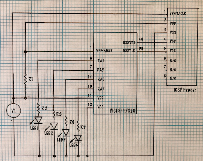
Bill of Materials
- R1 - 47KΩ
- R2 – R5 - 1KΩ
- LED1 – LED4 - HLMP-1719 or equivalent
- V1 - 3.3V source
Software
Version 6.00 of the MPLAB® X Integrated Development
Environment and MCC plugin version 5.4.11 were used to develop the
application. The screenshots that follow were taken from the
Windows version of these tools. While the flow should be
similar across versions, some specific screen details or options
may appear different in newer versions of the IDE, the
associated plugins, and processor packs.
Creating the MPLAB X Project
A quick summary of the steps to creating a new MPLAB X project
for the PIC18F47Q10 is provided below; for more details around the
steps to create a project and even installing the IDE if you have
not yet done so, please see the
first post in this series. Launch the MPLAB X IDE to get started.
- Select a new project of type Standalone Project
- Select the correct device – this post is using the 8-bit PIC18F47Q10.
- Select the tool you will be using for programming / debugging – this post is using a PICkit 4 in circuit debugger
- Select the latest version of the 8-bit compiler installed on the development workstation
- Enter a project name – this post named the project GPIOProgramming
Once the project is created, ensure Use low voltage programming
mode entry
is selected (project Properties / PICKit4 / PICKit4
Tool Options) – if this is not selected,
processor damage can
result
!
For the debugger / programmer tool to appear in the drop down it
must be connected to the workstation and recognized by the IDE.
Configuring the Internal Oscillator
A quick summary of the steps to configure the processor's internal
oscillator through MCC (MPLAB X Code Configurator) appears below. For additional details
and step by step screen captures of getting MCC set up and running
and configuring the internal oscillator please review the
first post in this series
- Launch MCC from the IDE toolbar
- Select MCC Classic Content Type
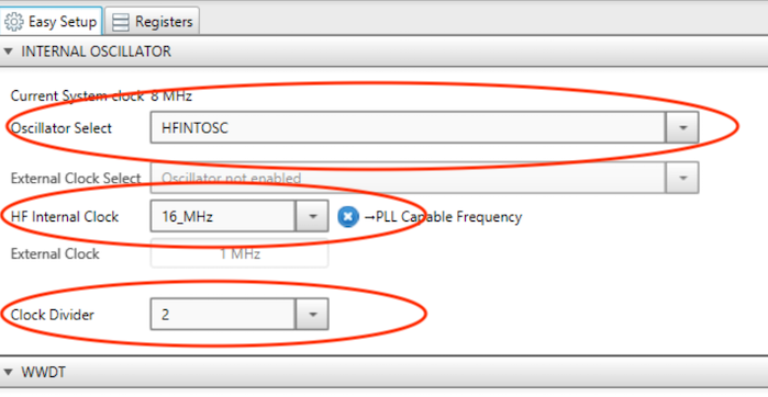
- Configure the clock source for the project to be 8MHz driven by the high frequency internal oscillator.
The System Module configuration should appear as:
The first post in this series also used MCC to configure RA4 as a GPIO output. This application configures the four GPIO output pins via application code therefore that configuration from the first post is not needed for this application.
Once the Internal Oscillator configuration is set, generate the code for the current configuration.
Adding the GPIO Management Source
The main source file, main.c, is where the GPIO initialization
code is placed. Choosing to add the code to main source file
is a matter of preference. The code could be placed in its
own header / source file structure similar to how MCC generated
code is structured in the project. That header would then be
pulled into the main source file with the GPIO initialization
method called prior to entering the application loop. It is
not advised to add any code to any of the generated MCC as the
changes could be lost if the MCC sources are ever re-generated.
main() Structure
The main source file contains some include files and a single function, main(). The header files include the necessary definitions and MCC generated files as discussed in the second post of this series. The main() function is the entry point of the application.
void main(void)
{
    // Initialize the device
    SYSTEM_Initialize();
    // If using interrupts in PIC18 High/Low
Priority Mode you need to enable the Global High and Low
Interrupts
    // If using interrupts in PIC Mid-Range
Compatibility Mode you need to enable the Global and Peripheral
Interrupts
    // Use the following macros to:
    // Enable the Global Interrupts
    //INTERRUPT_GlobalInterruptEnable();
    // Disable the Global Interrupts
    //INTERRUPT_GlobalInterruptDisable();
    // Enable the Peripheral Interrupts
    //INTERRUPT_PeripheralInterruptEnable();
    // Disable the Peripheral Interrupts
    //INTERRUPT_PeripheralInterruptDisable();
    while (1)
    {
        // Add your application code
    }
}
The structure of main() invokes any one-time call functions – typically associated with application initialization and configuration - and then enters an infinite loop. This infinite loop is the primary processing loop for application code. Exiting the loop halts application execution until the processor is reset resulting in the main() function executing again.
MCC inserts a one-time call to the SYSTEM_Initialize() resulting in initializing the system to the state specified through the MCC plugin.
SYSTEM_Initialize() in turn calls the following functions:
- PMD_Initialize() – enables / disables processor peripherals
- PIN_MANAGER_Initialize() – sets up the GPIO registers and other pins to the configuration specified via the MCC plugin.
- OSCILLATOR_Initialize() – updates the oscillator / clock configuration to that specified through the MCC plugin.
Optional Project Configuration and Clean Up
MCC generates commented place holders in main() for interrupt configuration. As this
application does not use interrupts, those commented
placeholders can be safely removed.
Setting up GPIO Initialization
Forward declare the method to initialize the GPIO registers. The declaration is placed anywhere prior to the main() function implementation. The GPIO initialization function implementation follows the main() function implementation.
The initialization function, GPIO_Initialize(), is called immediate after SYSTEM_Initialize(). The name GPIO_Initialize was subjectively chosen to follow the MCC generated function names. The main source appears as:
#include "mcc_generated_files/mcc.h"
/*
Main application
 */
void GPIO_Initialize(void);
void main(void)
{
    // Initialize the device
    SYSTEM_Initialize();
    GPIO_Initialize();
    while (1)
    {
        // Add your application code
    }
}
void GPIO_Initialize(void)
{
}
/**
 End of File
*/
GPIO Initialization
The GPIO configuration needed for the project circuit is:
- RA4 (PDIP 40 Pin Package – Pin 6) output – initial state logic level 0
- RA5 (PDIP 40 Pin Package – Pin 7) output – initial state logic level 0
- RA6 (PDIP 40 Pin Package – Pin 14) output – initial state logic level 0
- RA7 (PDIP 40 Pin Package – Pin 13) output – initial state logic level 0
The GPIO_Initialize() function implementation appears as:
void GPIO_Initialize(void)
{
    ANSELA |= 0xF0;
    TRISA &= 0x0F;
    LATA &= 0x0F;
    WPUA &= 0x0F;
    ODCONA &= 0x0F;
    SLRCONA |= 0xF0;
}
Eight registers were discussed previously but only six registers are set. As the four pins on PortA need to be configured as output, the PORTX and INLVLX registers are not used as they are only used when the pins are configured as inputs.
Each register is accessed by the name in the datasheet – this is possible as the included header file for the target processor - pic18f47q10.h – contains the definition, for example, ANSELA
#define ANSELA ANSELA
extern volatile unsigned
char
ANSELA
__at(0xF0C);
This matches with the datasheet that documents the ANSELA SFR address is 0xF0C:
For more information of how the pic18f47q10.h header is included
in the project, please see the second post in this series
Modifying & Preserving Register Contents
A good technique when manipulating SFR values is to only modify the relevant values while leaving the other bits of the register undisturbed. The operation should also be efficient such as applying a single bit mask to the register to make the changes in a single operation.
In order to set the values needed, bits within the register need to be either set to logic high, 1, or logic low, 0. Turning to Boolean algebra, the null element theorem can be applied to set a bit, or set of bits, to either 1 or 0. The null element theorem is described by an operation that when performed with a constant value results in that constant regardless of other values in the equation. The null element theorem is expressed by the following equations:
$$ B \bullet 0 = 0 $$
and the dual:
$$ B + 1 = 1 $$
With the ability to force a bit to a specific value, all that is left is to ensure the other bits in the register are not altered. Again looking to Boolean algebra, the identity theorem is described by an operation that when performed on a variable yields itself. The identity theorem is expressed by the following equations:
$$ B \bullet 1 = 1 $$
and the dual:
$$ B + 0 = B $$
An example of putting these concepts into practice, the program calls for the four pins associated with the upper nibble of port A to be digital output. To disable analog functionality for those pins, the four bits of the upper nibble of the ANSELA SFR need to be set to logic level 1. ORing a bitmask of 0xF0 forces the upper nibble to 1111b while preserving the current value of the lower nibble:
ANSELA |= 0xF0;
The |= operator is short-hand for
ANSELA = ANSELA | 0xF0;
This results in a read-modify-write operation on the ANSELA register.
The design calls for all four outputs start in a logic low (0) state. As the pins are outputs, the upper nibble of the Latch A register needs to be set to 0 while the lower nibble should not be altered. Following the previously discussed approach, ANDing the port with a 0x0F mask will populate the latch register with the required values.
LATA &= 0x0F;
Similar logic is applied to the remaining registers to complete the configuration.
Modifying Single Bits
The Microchip supplied header files also provide constructs to alter individual bits:
ANSELAbits.ANSELA7 = 1;
Using this approach, each bit of the upper nibble could be set without using a bitmask with AND / OR operations. However, each bit update is a individual read-modify-write. In this case, one operation – the AND / OR with the bitmask, replaces four individual operations. Using the individual bit method is convenient if there is only one bit in the register being modified – such as a status bit that perhaps turns a peripheral on or off.
Defensive Programming
Even when there is no GPIO configuration specified via MCC, code is generated to initialize all the ports’ registers to the default value specified in the data sheet. This is easily verified viewing the PIN_MANAGER_Initialize() method in pin_manager.c. The function sets all registers for every port. In both cases, the default value of the upper nibble of the LATA and ANSELA registers just happen to match the values the application needs. Setting those values again in the GPIO_Initialize() function seems wasteful. Even if PIN_MANAGER_Initialize() is removed or not called for whatever reason, the application can still fallback on the default value of those registers on processor start up, correct? A programming best practice is to not make assumptions – such as assuming the default values have not been modified by another function somewhere, or assuming that a method in a generated file, PIN_MANAGER_Initialize() is being called appropriately at the correct time. This application is simple enough that the high-level flow is easy to see and verify that the expected functions are being called in the correct order. Consider however, as the application expands in scope and there is now peripheral initialization for a few timers, a serial port, two SPI devices and an I2C device. Perhaps each peripheral is managed through separate header / source files and simply included and invoked with the main.c source file. Knowing that there is a specific function written and called for configuring those four GPIO pins significantly reduces the chances of errors and the modularity makes both maintaining existing functionality as well as adding new features easier.
The code also took specific actions to only modify the minimum number of bits. A read-modify-write operation was incurred with each registry update, the entire register could have simply been set with a single write command such as:
LATA = 0x00;
Consider when another function within the application may need to configure that lower nibble with a different value, perhaps they may need to be configured as inputs or as analog functions. Consistently applying the practice of only modifying the necessary bits of a register ensures that the current function does not overwrite values set by another function and functions called after the current function do not overwrite the values being set. As previously stated, with an application of this size and complexity this approach can certainly seem excessive – however, consistently applying best practices regardless of current application size or complexity is itself a best practice!
Toggling the LEDs
The necessary configuration is in place to initialize the GPIO ports; the four LEDS start in an off state. Turning back to the main() function, within the infinite loop logic can be added to toggle the state of the LEDs at the required interval. The Microchip compiler provides a suite of “builtin” functions – one of them being __delay_ms() – which is actual a #define for the actual function _delay() that conveniently takes an unsigned long argument for the number of milliseconds to delay. This does require definition of the symbol _XTAL_FREQ which MCC placed in the generated device_config.h header file.
After a one second delay completes, the state of the output pins needs to toggle. This could be done by reading the current value and using some conditional logic to determine what the next value should be. However, this can also be completed with a simple XOR operation. Looking at an XOR operation truth table, XORing a value with 1 toggles the value:
| Initial Value | Modifier | Result |
|---|---|---|
| 0 | 1 |
1 |
| 1 | 1 |
0 |
And in keeping with the concept of only modifying the relevant
bits in the register, XORing any value with 0 does not change the
original value:
| Initial Value | Modifier | Result |
|---|---|---|
| 0 | 0 | 0 |
| 1 | 0 | 0 |
As the upper nibble of the port A is set up as outputs, the values need to be updated in the LATA register. The implementation of main() should appear as:
void main(void)
{
    // Initialize the device
    SYSTEM_Initialize();
    GPIO_Initialize();
    while (1)
    {
        __delay_ms(1000);
        LATA ^= 0xF0;
    }
}
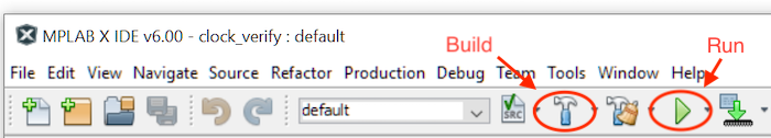
Building and Running the Application
The project can now be built, uploaded to the microcontroller, and run. The Run button on the toolbar both builds and if the build succeeds, programs the processor. I prefer to keep the two as separate operations and almost always click Build and then Run (which builds the application again!). The related buttons are highlighted below:
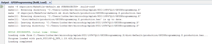
Regardless of how you get there, you should see both a build output:
And a load output...
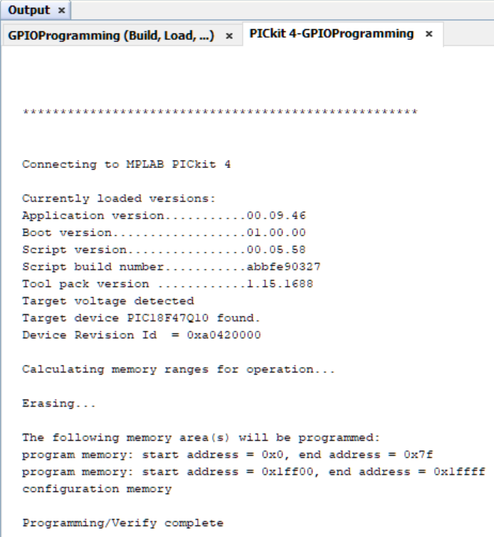
Once upload is complete, the four LEDs begin blinking.
Final Thoughts
The implementation in this application is not very efficient. The application cannot perform any additional work while the LEDs are either lit or dark. This is due to the a function call to implement the delay; the processor is either waiting in the delay function or toggling the LATA register values – it cannot do anything else.
An application that does nothing but toggle LEDs is not very useful. Typically a flashing LED is just part of a larger application – perhaps the LED is indicating activity such as an error, a power state, waiting for input, etc. The LED is only a small piece of a much larger application.
The next post in this series takes a step to address how the processor can be freed up for other work while still controlling the LED display. This involved the introduction of a hardware timer peripheral to handle the timing of the LED toggle. The application will still need to poll that peripheral to determine when the LEDs should be toggled, however, in between polls the processor can perform other limited tasks. The final element to completely move the timing outside of the main application, an interrupt, is introduced in the last post of the getting started series. Implementing an interrupt frees the processor to perform other tasks and only process updating the LED state when the current application is interrupted to handle time period expiration.
Summary
This post started with an overview of the PIC 8-bit GPIO ports followed by a dive into the eight individual SFRs used to configure and manage the five ports available on the 40 pin package of the PIC18F47Q10. Additional discussion covered when to use the LATx (LATch) register vs the PORTx register for managing the values of the related pins in the port. Next a new circuit was introduced expanding on the circuit built in the first post of this series, still using a discrete PIC18F47Q10 programmed with a MPLAB PICkit 4 programmer/debugger on a breadboard. With the circuit built, a simple application was implemented providing an example of configure the upper nibble port A as digital outputs to drive the LEDs. Finally, code was introduced to flash the LEDs at a frequency of 0.5Hz.


- Comments
- Write a Comment Select to add a comment

The TRIS register is a classic trap for developers who are familiar with other MCUs and are used to "0" being "input" and "1" being "output". Any text discussing this register should be in bold red :-)
Thank you for this comprehensive post series; it's a great resource for first-time PIC users.
To post reply to a comment, click on the 'reply' button attached to each comment. To post a new comment (not a reply to a comment) check out the 'Write a Comment' tab at the top of the comments.
Please login (on the right) if you already have an account on this platform.
Otherwise, please use this form to register (free) an join one of the largest online community for Electrical/Embedded/DSP/FPGA/ML engineers:


